Stackup Overview
Stackup is the soul of Multi-layer PCB.it refers to the arrangement of copper layers and insulating layers that make up a PCB prior to board layout design.Stackup information includes the layers order,which is layer 2,,which is layer 3.Many customers sent us gerber file without stackup or layer order information. That means we can not proceed the PCB. If you do not have customs stackup ,you also need to provide layers information to PCB manufacturers.
Here is an example. TOP/inner 1/Plane1/Bottom,or CMP/LY2/L15/Bottom. So we can know inner 1 or LY2 is layer 2. The core material and Prepreg is flexible for us to meet the final thickness.
Here is an example. TOP/inner 1/Plane1/Bottom,or CMP/LY2/L15/Bottom. So we can know inner 1 or LY2 is layer 2. The core material and Prepreg is flexible for us to meet the final thickness.
Another important information is one core for 4 Layer PCB,2 cores for 6 layers PCB and 3 cores for 8 layers PCB.The dielectrical (Prepreg)thickness should not be more than 0.3mm, otherwise, we have to use more than two Prepreg material with higher cost.
|
|
The above information is very helpful for any PCB factories,it helps us to understand the layers order and the stackup.We prefer you to specify the PCB layers order and stackup information in the gerber too.
Standard PCB stackup
Standard PCB stackup is for the normal PCBs without impedance or high-speed requirements,it is not critical but to meet the final thickness.Below is an example for standard FR4 PCB ,4 layer with 1.6mm thickness.
|
Standard 4 Layer PCB with one core
4 Layer PCB with one core to stackup is standard stackup.
Layer 2 and Layer 3 is in the same core. |
4 Layer PCB with two cores customs stackup
4 Layer PCB with two cores is customs stackup.Layer 1 and Layer 2 is in the first core ,Layer 3 and Layer 4 is in the second core. The PCB is made like a 6 layer.
|
Impedance PCB stackup
Impedance PCB usually have customs stackup,it specifies the trace width,space in gerber. Then,the most important is the stackup ,it may change the final result.Usually, there are two impedance types in PCB manufacturers.One is Singled-ended ,another is Differential impedance.However,there are many models for PCB factories to test the impedance. The impedance trace is in inner layer or out layer,solder mask or not, Coplanar or not. see our impedance PCB to get more information about impedance.Below are some models .
|
Outer layer—Single-ened type
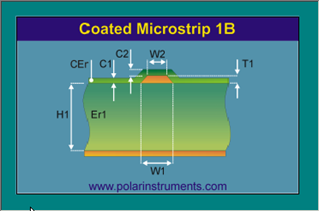
Application:Outer layer over solder mask H1: Dielectric thickness Er1:Material DK W1:Trace Width(bottom) W2:Trace Width(top) D1:Space from trace to ground T1:Copper thickness C1:soldermask thickness over raw material C2:solder mask thickness over copper CEr:Solder mask Dk Outer layer--Differential Type
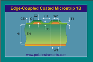
Application:Outer layer over solder mask H1: Dielectric thickness Er1:Material DK W1:Trace Width(bottom) W2:Trace Width(top) S1:Trace space T1:Copper thickness C1:soldermask thickness over raw material C2:solder mask thickness over copper C3:soldermask thickness over raw material CEr:Solder mask Dk |
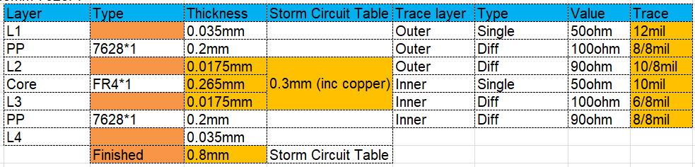
How to design a 4 layer impedance PCB with 0.8mm thickness?With more than 10 years experience, 50ohm and 100 or 90 ohm impedance PCB should be like this.Below is just an example,you can use different cores and PP to get different trace width.
Please contact us to get the impedance stackup table.
Please contact us to get the impedance stackup table.
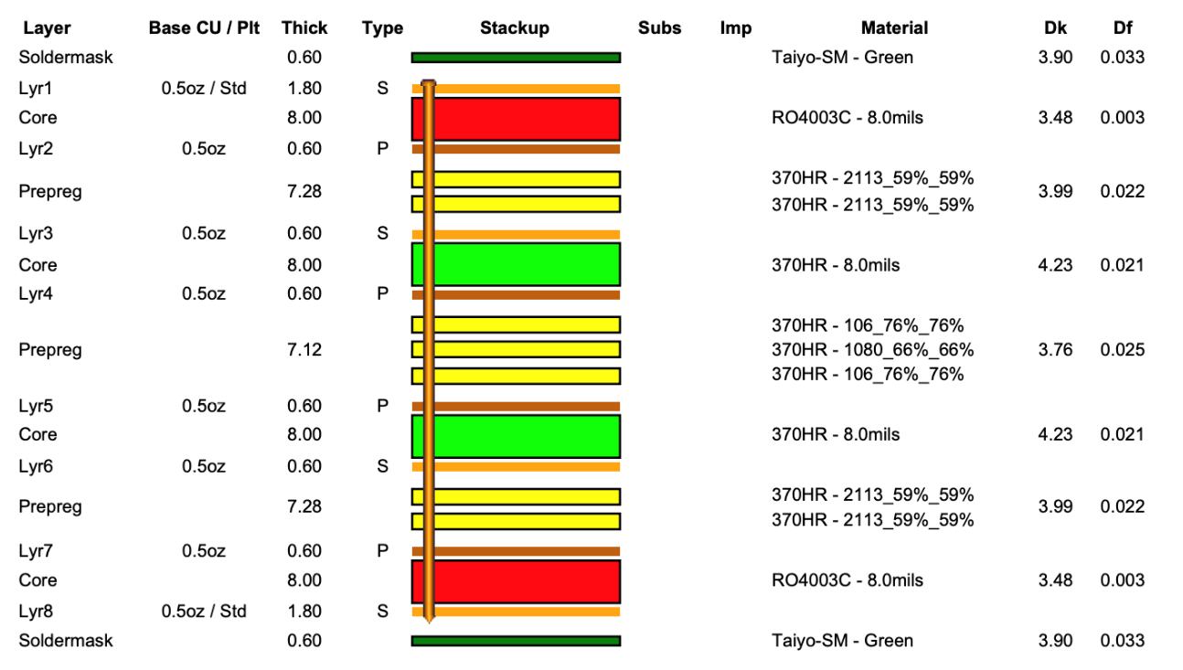
Hybrid stackup
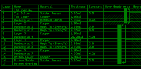
High frequency PCB usually made with Rogers material+FR4 or full Rogers material . here is an example of hybrid stackup.
6 layer, Rogers RO4350B+high TG FR4 material,blind vias from L1-L2,L2-L6.
Storm Circuit focus on such high frequency /RF /microwave material. We can make From single RF material layer to 12 layer.
RF material is different with FR4,many processes are different too. Storm Circuit can make many types hybrid material jobs with
blind/buried vias.
|
|
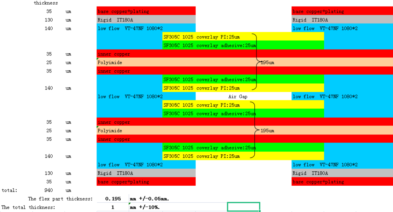
Rigid-flex stackup
Rigid-flex stackup is more complex. there are many types.
Below is an example we made ,it is a 6 layer rigid-flex PCB,1.0mm rigid part and 0.3mm flex part.
Below is an example we made ,it is a 6 layer rigid-flex PCB,1.0mm rigid part and 0.3mm flex part.