How to export Kicad PCB to gerber files
KiCad is an open-source software tool for the creation of electronic schematic diagrams and PCB artwork. Beneath its singular surface, KiCad can be considered mature enough to be used for the successful development and maintenance of complex electronic boards. It does not present any board-size limitation and it can easily handle up to 32 copper layers, up to 14 technical layers and up to 4 auxiliary layers. KiCad can create all the files necessary for building printed boards, Gerber files for photo-plotters, drilling files, component location files and a lot more. Being open source (GPL licensed), it represents the ideal tool for projects oriented towards the creation of electronic hardware with an open-source flavour.
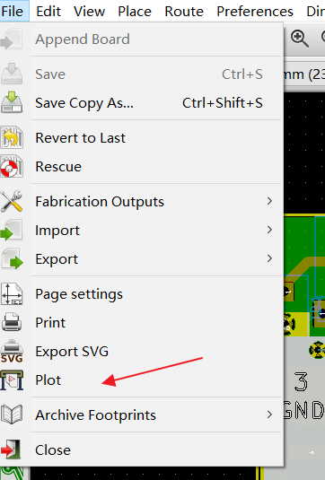
Generate Drill and Gerber FilesSelect File -> Plot from the menu to open the gerber generation tool.
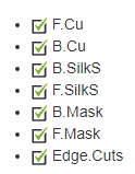
In general, there are 8x layers you need to have a PCB fabricated:
|
|
|
Drill file
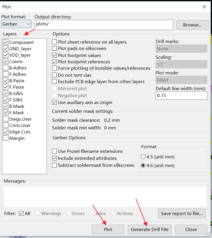
In the Plot window with the Plot format set for Gerber, be sure these Layers are checked: |
|
|
If you don't know which layers, please check all layers, Storm Circuit will help you to use the right layers.
Click ‘Plot’ to generate the gerber files for the layers. |
|
|
Don't forget to Generate the Drill Files.
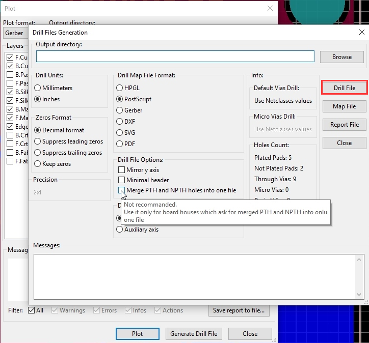
Click on ‘Generate Drill File’ button. You can use the defaults here as well. More on the PTH vs. PTH check box in a minute. For now just click ‘Drill File’ or press ‘enter’ to generate the drill file. Use the same output folder as for the gerbers, which should be the default. |
|
|
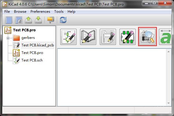
Check the Gerber files in GerbView
Next, click ‘Close’ to exit the Drill and Plot windows. All of the files should have appeared in your gerbers folder. KiCAD comes with a gerber viewer called GerbView, you can open the “GerbView” and check what your board looks like before sending it to manufacturer. |
|