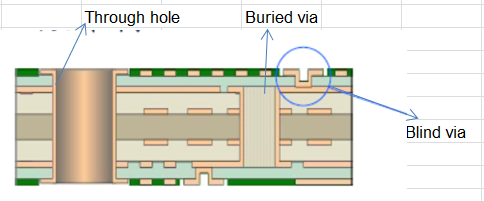
PCB blind and buried via
|
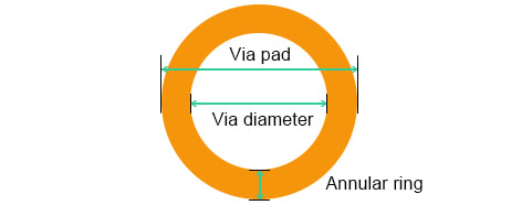
vias are small holes, usually,we say vias are holes less than 0.3mm.
Blind via is the via from top or bottom layer to inner layers, they are not through,we can see the vias from PCB top or bottom side. Buried via is the vias in the inner layers,we can not see these vias from PCB top or bottom side. Stacked vias are laminated blind or buried vias, multiple vias inside a circuit board built together around the same center |
|
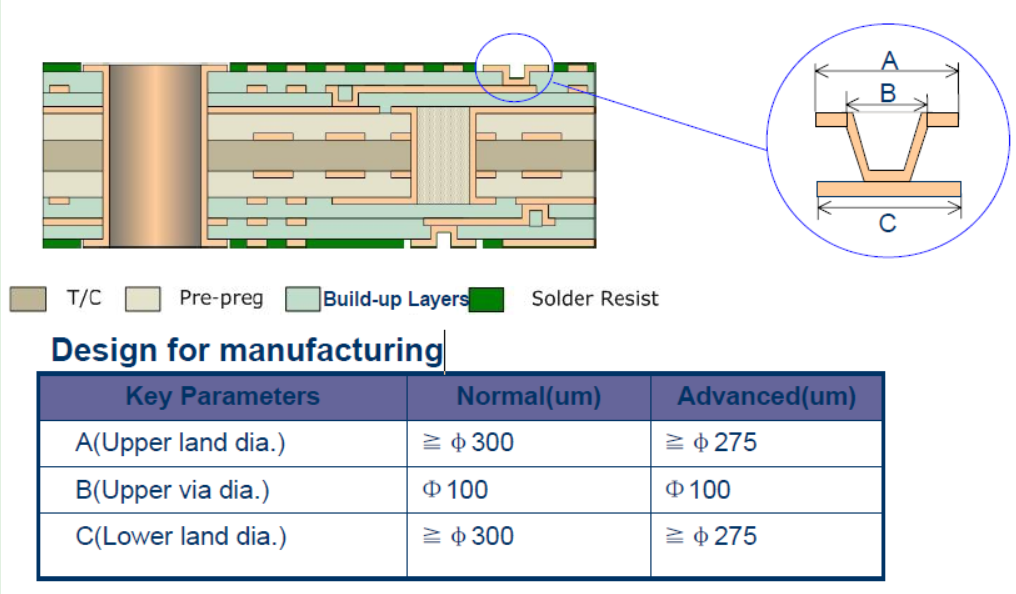
Blind and/or buried vias are usually for HDI design.less space,more components. Especially in the BGA area,the via in pad vias are also blind or buried vias.BGA will be loaded on the blind/buried vias,so these vias have to be filled and plated to flat.
|
Via Type Via Diameter(mm)
|
|
Non Stacked 2--HDI
|
Non Stacked 2--HDI
|
Stacked but Non Copper Filled 2--HDI
|
Stacked & Copper Filled 2--HDI
|