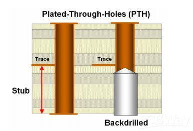
Back Drilling PCB
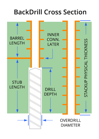
Backdrilling is a manufacturing technique used on high speed multi-layered boards to reduce the amount of parasitics generated by plated through holes.Backdrilling is one type of controlled depth drilling (CDD),the technology removes the STUBs (A stub is an unnecessary portion of the vias, which is like an antenna on the signal path and is a discontinuity of the impedance and produces reflections and EMC problems.)
Usually,if the signals speed>5GB/s,and layer counts >8,we advice our customer to design the PCB with backdrilling technology.
Stubs in Detail:As already mentioned, stubs interfere with the signal integrity of high-frequency circuit boards. Stubs cause unwanted resonant frequency nulls which appear in the insertion loss plot of the channel.
|
|
Backdrilling is a special craftsmanship of control depth drilling.
Advantages:
- Reduce interference of other signal
- Improve signal integrity
- Reduce partial plate thickness
- Reduce the use of blind and buried vias to reduce the difficulty of PCB fabrication
- cost effective than blind/buried technology
General Characteristics
- Mostly are rigid boards on back
- Normally used on 8 layers or above
- Board thickness is over 2.5mm
- Minimum hold size is 0.3mm
- Backdrill is 0.2mm larger than the vias
- Tolerance of backdrill depth+/-0.05MM