10 layer & 20 layer PCB
Usually,10 & 20 layers PCB are HDI board,but some are not .Some with big trace width and space,holes are over 0.3mm too. We have much experience in doing 10 layer PCB & 20 layer PCB.
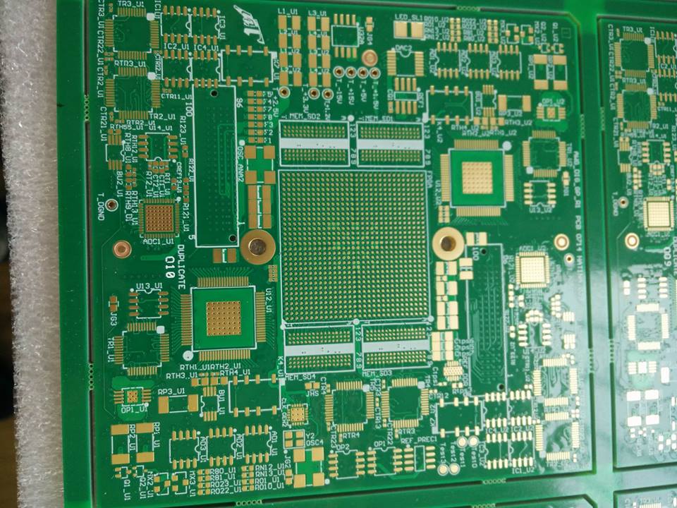
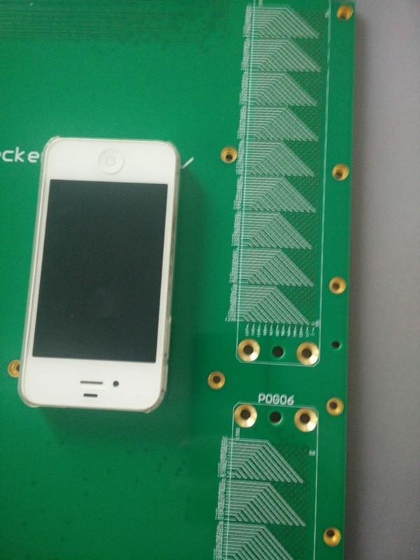
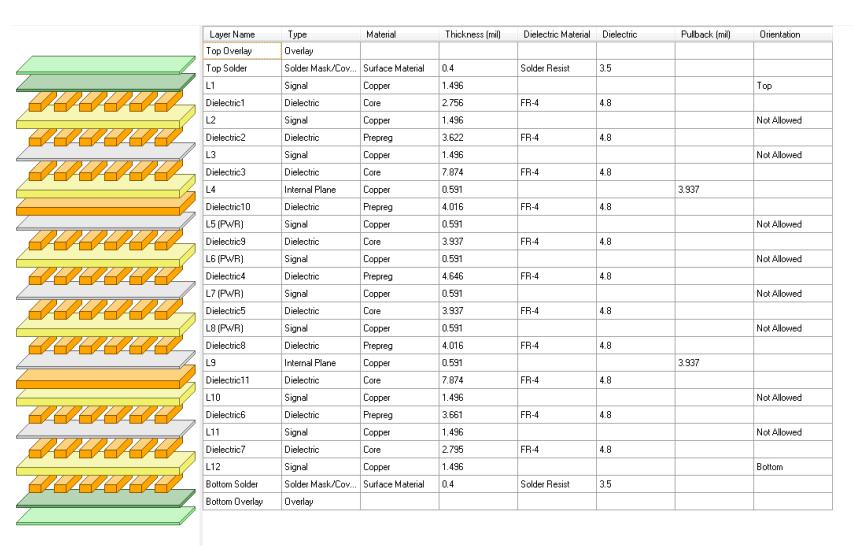
A ten-layer board should be used when six routing layers are required. Ten-layer boards, therefore, usually have six signal layers and four planes. Having more than six signal layers on a ten-layer board is not recommended. Ten-layers is also the largest number of layers that can usually be conveniently fabricated in a 0.062" thick board. Occasionally you will see a twelve-layer board fabricated as a 0.062" thick board, but the number of fabricators capable of producing it are limited.. High layer count boards (ten +) require thin dielectrics (typically 0.006" or less on a 0.062" thick board) and therefore they automatically have tight coupling between layers. When properly stacked and routed they can meet all of our objectives and will have excellent EMC performance and signal integrity. A very common and nearly ideal stack-up for a ten-layer board is shown in Figure 12. The reason that this stack-up has such good performance is the tight coupling of the signal and return planes, the shielding of the high-speed signal layers, the existence of multiple ground planes, as well as a tightly coupled power/ground plane pair in the center of the board. High-speed signals normally would be routed on the signal layers buried between planes (layers 3-4 and 7-8 in this case). Examples of what we did for 10 and 20 layer PCBs.
|
Download
Mullilayer standard stack upstackup.pdf PCB Fab check list PCB capability Sample BOM Flex PCB material High frequency material 
Original&New LPC178 chips
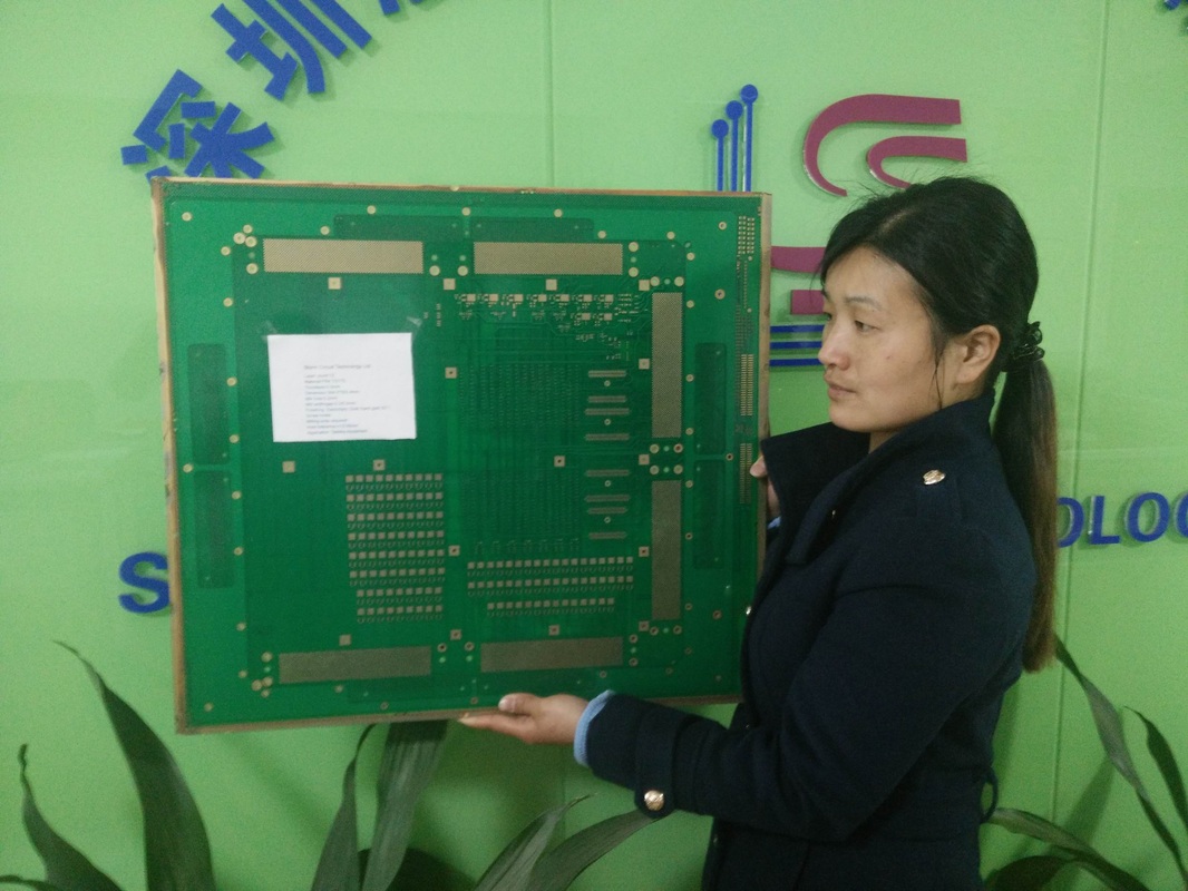
Our PCBs
Flex PCB Rigid-flex PCB RF board Heavy copper PCB 20 layer PCB 10 layer PCB HDI PCB ENEPIG PCB Control impedance Quick Turn boards MC PCB 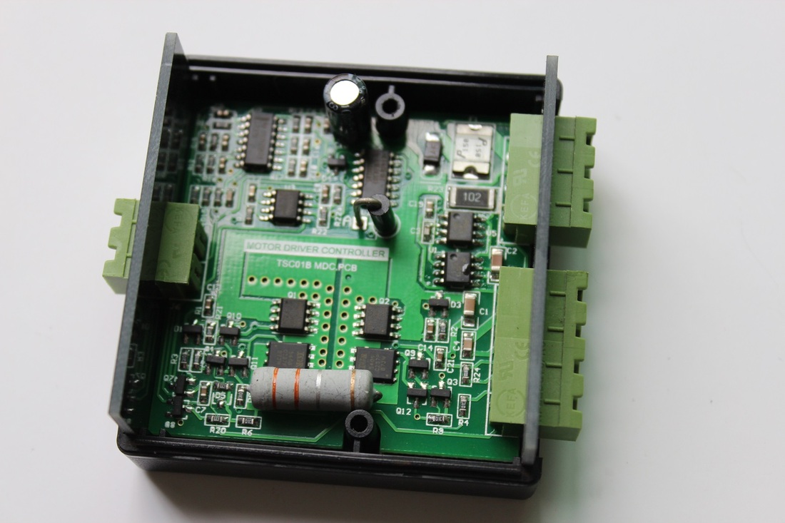
Turnkey assembly service
|
|
|